Samsung on Thursday announced that it has started production of EUV 7nm LPP chips, which is a very complex way to tell the world that 7nm chips will be ready in time for the Galaxy S10 launch next year. If 7nm sound familiar, that’s because smartphone makers including Huawei and Apple have already launched such devices. Huawei was the first to unveil the 7nm Kirin 980 that powers the Mate 20 Pro, but Apple’s 7nm A12 Bionic chip in the iPhone XS and XR models shipped to consumers first.
So what does EUV 7nm LPP means, or 7LPP means? It’s short for “7-nanometer (nm) LPP (Low Power Plus) with extreme ultraviolet (EUV) lithography technology.” 7nm chips will be faster and more efficient than the 10nm chips that power most of the 2018 Android flagships, Samsung’s Galaxy S9 and Note 9 included.
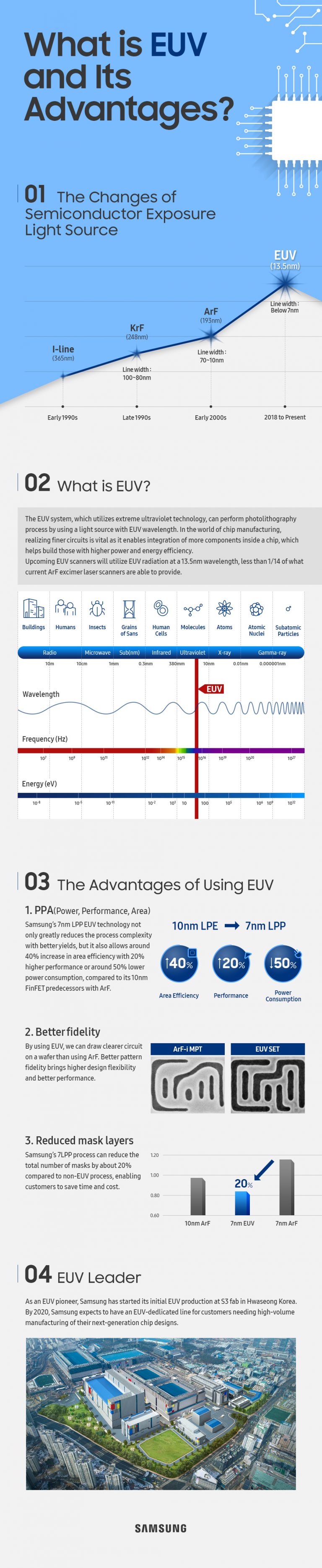
But what’s interesting about EUV tech, according to Samsung, is that it can reduce the manufacturing cost of these chips:
EUV uses 13.5nm wavelength light to expose silicon wafers as opposed to conventional argon fluoride (ArF) immersion technologies that are only able to achieve 193nm wavelengths and require expensive multi-patterning mask sets. EUV enables the use of a single mask to create a silicon wafer layer where ArF can require up to 4 masks to create that same layer. […]
Compared to its 10nm FinFET predecessors, Samsung’s 7LPP technology not only greatly reduces the process complexity with fewer layers and better yields, but also delivers up to a 40% increase in area efficiency with 20% higher performance or up to 50% lower power consumption.
Samsung doesn’t mention the name of the 7nm Exynos chip that will power the Galaxy S10 next year or the Galaxy S10 in the press release. But it’s very likely that Samsung’s own 7nm chip tech will be used to supply the processors next-gen Galaxy flagships will require.
It’s interesting to note that TSMC a few days ago also announced (via ExtremeTech) that it’s going forward with its own 7nm EUV plans. TSMC is one of Samsung’s biggest rivals and the world’s most important chip makers. It’s also the company that exclusively manufactures A-series chips for Apple, including the 7nm A12 Bionic. But the A12 isn’t built on EUV tech — AnandTech explained TSMC’s existing 7nm earlier this year:
TSMC’s CLN7FF process technology will rely on deep ultraviolet (DUV) lithography with argon fluoride (ArF) excimer lasers operating on a 193 nm wavelength. As a result, the world’s largest contract maker of semiconductors will be able to use existing manufacturing tools to make 7 nm chips. Meanwhile, to keep using DUV lithography the company and its customers have to use multipatterning (triple and quadruple patterning), which increases design and production costs as well as product cycles.
TSMC is expected to manufacture the 7nm Snapdragon 855 next year, which should be renamed to Snapdragon 8150 according to reports. That’s the chip that will power some Galaxy S10 and Note 10 versions this year.
Regardless of the technology used, 7nm chips should offer similar performances, although don’t expect Samsung’s 7nm Exynos chips to beat Apple’s A12. But EUV will make it cheaper for companies to mass produce it.
Finally, the following infographic, also from Samsung, briefly explains its 7nm chip innovations: